Getting Started with FPGAs and Cx - Altera Edition
Alan Kay said, "People who are really serious about software should make their own hardware." Not sure that I agree, but I'm definitely a software engineer who likes to make his own hardware. This tutorial will lay the foundations for hardware design using relatively low-cost tools.
Why design your own hardware? A few possible reasons:
- It gives you more flexibility to create what you want
- Algorithms implemented in hardware are typically faster and/or more energy efficient than the same algorithm in software
- It's yet another outlet for creativity, and creating stuff is fun
This tutorial's goal is incredibly simple; design something that flashes an LED. Keeping it simple will give us results fast, despite having a lot to learn.
NOTE: This is a rewrite of an earlier tutorial to use an Altera FPGA based development board. I switched development kits after having serious software issues. So, I've restarted the tutorial series from scratch.
The Tools
Hardware is designed with the help of specialised software. There's a mind-boggling array of options and we're going to use a hardware design language called Cx. It's designed specifically "to bring digital hardware design within reach of any developer," which sounds great!
We also need a way to test the designed hardware. This used to be a very expensive and time-consuming process. Thankfully, Field Programmable Gate Arrays (FPGAs) make this much easier and cheaper. FPGAs are chips containing a large array of logic gates (the building blocks of digital circuits). These gates can be connected up in many different ways thanks to a set of programmable interconnections. This allows us to upload our hardware design into the FPGA, and run it using real logic. Even better, the chip is reprogrammable, so if something doesn't work as intended, then we can fix the design, generate a new "bitfile," and upload the new design to the chip.
What You'll Need
There are a few things that you'll need:
- A computer capable of running the necessary software
- An internet connection to download the software
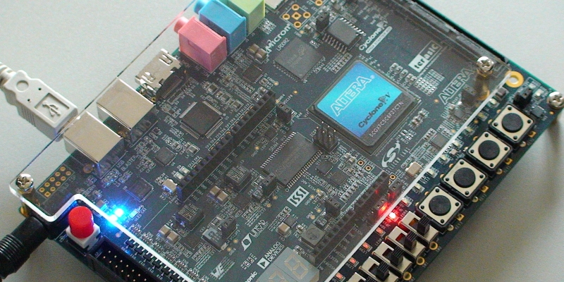
- A Cyclone V GX Starter Kit FPGA (C5G starter kit) or something similar
NOTE: Non-Altera boards are fine too, but you'll have to figure out some stuff on your own - A willingness to learn, and some persistence
It'll also help a lot if you have programming experience (especially in C, Java, or hardware languages such as Verilog and VHDL). Failing that, an understanding of boolean logic is highly recommended.
Step One: Installing the Software
You will need to download and install the following:
- ngDesign (the Cx code editor and compiler): https://www.synflow.com/download
- Altera Quartus (for generating FPGA bitfiles): http://dl.altera.com/?edition=lite
IMPORTANT: Be sure to get the free lite edition
NOTE: If you're using an FPGA made by Xero or Lattice, then you'll need to download their software instead - Download any support material for your development kit (manuals, constraints files, tools, etc.)
Cyclone V Starter Kit Resources: http://www.terasic.com.tw/cgi-bin/page/archive.pl?Language=English&CategoryNo=165&No=830&PartNo=4
NOTE: Be sure to get the user manual and System CD
Step Two: Set Up the Project
Start ngDesign. The first time round it will ask you where to put your workspace. Create a workspace wherever you like. Next, right-click in "Project Explorer" (ngDesign's left column), and select New => Synflow Project. Call the new project LEDFlasher.

NgDesign stores source files in "packages" (rather like Java does). Within the new LEDFlasher project is a "src" directory, right-click on that, ans select New => package. Create a new ledflasher package. Synflow (Cx's creator) recommends naming packages using Java's convention, so I'll name mine "com.keasigmadelta.ledflasher". Replace "com.keasigmadelta" with whatever you wish.
NOTE: The naming convention makes it easier to use code from multiple people/organisations in the same design. Don't get hung up on the naming; you can always change it later.
Step Three: The Design
As I said earlier, we're designing a simple LED flasher circuit. The circuit is structured as follows:
")
The clock divider takes an input clock, and divides it to produce two pulses per second (so a 2 Hz clock/enable signal). This 2 Hz signal is then input into "ledDriver" which toggles the LED on and off once per second.
NOTE: The clock and reset signals have been left off the block diagram above for simplicity.
Create the LEDDriver Task
Cx divides circuits/processes into multiple tasks. These tasks are connected together in networks. So, lets create the first task, the LEDDriver. Right-click on the "ledflasher" package that was created in Step Two above, and select New => Cx Task. Call this task LEDDriver.
NgDesign will create a skeleton task for you. Enter the following code:
package com.keasigmadelta.ledflasher;

task LEDDriver {
	// Enables toggling the LED's state
	in bool toggle;

	// output to the LED
	out bool led;

	// The LED's current state
	bool ledState;

	void setup() {
		ledState = false;
	}

	void loop() {
		if(toggle == true) {
			ledState = !ledState;
			led.write(ledState);
		}
	}
}
Let's go through the important additions. First, we declare an input signal called toggle, and an output signal called led:
// Enables toggling the LED's state
in bool toggle;

// output to the LED
out bool led;
These are both booleans, which mean that they can be either true, or false (a.k.a., a 1, or 0). The input (toggle) receives the pulse from the divider task, while the output (led) will drive an LED.
Next, we have a task variable called ledState:
// The LED's current state
bool ledState;
This stores whether the LED is currently on (true/1), or off (false/0).
The setup() function sets the LED's initial state to off:
void setup() {
	ledState = false;
}
Next comes the loop() function. This is the task's core, and is "executed" continually:
void loop() {
	if(toggle == true) {
		ledState = !ledState;
		led.write(ledState);
	}
}
In plain English, this code says: if the toggle input is true, then set ledState to the opposite of what it is now (!ledState means "not ledState"). Finally, write ledState to the led output.
NOTE: Digital circuits are kept in step using a clock. The clock signals when variables (a.k.a., registers) can change state. Cx tasks implicitly use a clock, so the loop() code above is executed every clock cycle.
Create the Clock Divider
The LED driver needs something to drive its toggle input. Since the C5G starter kit's clock runs at 50 MHz (50 million cycles-per-second) and we want the LED to flash once per second, we need something to slow it down. That's a job for a counter/divider.
Create a new task called Divider. Enter the following code:
package com.keasigmadelta.ledflasher;

task Divider {
	typedef u25 ClkCounter_t;
	const unsigned CLOCK_FREQ = 50000000; // 50 MHz
	const unsigned TARGET_FREQ = 2; // 2 Hz
	const ClkCounter_t DIVIDER = CLOCK_FREQ / TARGET_FREQ;

	// The output signal
	out bool enable;

	// The internal counter
	ClkCounter_t counter;

	void setup() {
		counter = 0;
	}

	void loop() {
		if(counter == DIVIDER) {
			// Send an enable signal (for 1 clock cycle)
			enable.write(0b1);

			// Reset the counter
			counter = 0;
		} else {
			// The enable signal is normally 0
			enable.write(0b0);

			// Increment the counter once each clock cycle
			counter++;
		}
	}
}
This task will count up to DIVIDER clock cycles, and then set the output enable to 1 (true) for one clock cycle. The target frequency (TARGET_FREQ) is set to 2 Hz, which will signal LEDDriver to switch the LED on (pulse one) and off (pulse two) once per second.
Some key things to look at in the code above:
- CLOCK_FREQ is the input clock frequency. If you're using another board, then you'll have to adjust this
- The line "typedef u25 ClkCounter_t" sets ClkCounter_t to be an unsigned integer that's 25 bits wide. This can hold values from 0 through to 225 - 1 = 33,554,432
IMPORTANT: If your development board uses a faster clock, then make sure that the counter is large enough to hold the value of DIVIDER. If in doubt, change "u25" to "u32." This will ensure that the counter is large enough. The FPGA synthesizer will trim away the unnecessary extra bits (and spit out warnings) - You may notice that the code uses "counter == DIVIDER." Software developers generally use >= (greater than or equals) just in case the number gets corrupted. However, in hardware design, an equals comparison (i.e., ==) uses less logic than >=, <=, >, or < comparisons. Less logic means a smaller and faster design, and that's a good thing
Connecting the Tasks Together in a Network
Now it's time to connect the individual tasks together to create a full circuit. Right-click on your ledflasher package, and select New => Cx network. Call the network LEDFlasher.
The code is as follows:
package com.keasigmadelta.ledflasher;
import com.keasigmadelta.ledflasher.LEDDriver;
import com.keasigmadelta.ledflasher.Divider;


network LEDFlasher {
	// One output, to the LED that we're flashing
	out bool led;

	// Need one divider
	divider = new Divider();

	// Create an LED driver, and connect it to the divider
	ledDriver = new LEDDriver();
	ledDriver.reads(divider.enable);

	// Connect the LED's output to led
	this.reads(ledDriver.led);
}
In brief, the LEDFlasher network has one output called led.
// One output, to the LED that we're flashing
out bool led;
The code creates one Divider and one LEDDriver:
// Need one divider
divider = new Divider();

// Create an LED driver, and connect it to the divider
ledDriver = new LEDDriver();
The Divider's enable output is connected to the LEDDriver's toggle input:
ledDriver.reads(divider.enable);
Finally, the LEDDriver's output (led) is connected to the led output:
// Connect the LED's output to led
this.reads(ledDriver.led);
That's it! Everything is connected.
NOTE: In Cx the clock signals are connected by default, so we don't need to write code that connects them. Cx tasks/networks also have an implicit reset signal called reset_n.
Why Use an "Enable" Signal Instead of Dividing the Clock Directly?
You may be wondering, why not feed the divided clock straight into the LEDDriver's clock input. After all, it's also a clock signal and using an enable signal looks like overkill. While that's true for this very simple design, having separate clock signals in a design requires careful synchronization between the parts that are clocked differently. Otherwise ugly problems can occur. I had a sigma-delta DAC design generate a lot of random noise due to this exact problem. One clock reached the DAC just as its input signals were switching, leading to random results.
The bottom line is, unless there's a very good reason for having multiple clocks, it's better to use one global clock for all logic and use "enable" signals to run different parts at different speeds.
Step Four: Generate Verilog Code
Alters's circuit synthesis software doesn't understand Cx, so we need to convert our Cx code into Verilog (or VHDL). NgDesign has a compiler that does this for us. Right-click on LEDFlasher in the project explorer (in the left-column), and select Run As => Hardware on FPGA.

Since this is the first time that we run the compiler, it will pop up a configuration dialog. Set the "Target Vendor" to Altera (or the vendor for your board's FPGA)

Next, click the "Run" button. This will generate the Verilog code.
Step Five: Synthesizing the Hardware
We're finally ready to take our design, and turn it into hardware. At this point we have to switch to Altera's Quartus. NgDesign has taken us as far as it can. Future versions will hopefully be able to synthesize hardware directly, but right now it can't (as at version 0.84).
Setting Up the Hardware Project
Terasic provide a convenient tool to generate new projects called System Builder. It's on the starter kit's System CD which you downloaded earlier. So, run the System Builder (C5G_SystemBuilder.exe). We'll only be using a clock signal, one LED, and the reset button, so select the following: CLOCK, LEDx18, BUTTONx4. Make sure that everything else is deselected, as shown below.

Click on the "Generate" button. It'll ask where to put the project file. I suggest creating a subdirectory called LEDFlasher_C5G within the projects directory.
NOTE: Other development boards may have a template in Quartus which can be used via the project wizard (File => New Project Wizard).
Open the new project in Quartus. Now, add the generated files to the project as follows:
- Select Project => Add/Remove Files in Project from the menu
- Click on the "..." button (to the right of the "File name:" field)
- Navigate to the source files within LEDFlasher/verilog-gen, and add them to the project
The end result should look like this:

Wiring the LED Flasher to the FPGA's I/O Pins
The next step is to connect our design to the FPGA's I/O pins. We're going to do this by changing the top level verilog file to LEDFlasher.v, and renaming the pins. That way we can design the entire circuit in Cx. Otherwise we'd have to learn a bit of verilog or use a schematic editor. Why add more things to learn when it's not needed?
At the top of the Project Navigator (left column of window) is a dropdown saying "Hierarchy." Click on it, and select "Files" from the dropdown:
 Right-click on LEDFlasher.v, and select "Set as Top-Level Entity" (Ctrl+Shift+V), as shown below.
 The top-level entity is another name for the design's root. It's the part that connects to the outside world. Everything else is inside it.
NOTE: It's a good idea to delete the LEDFlasher_C5G.v that System Builder generated, as we won't be using it.
The next task is renaming the pins to match the signals in our design. From the menu, select Assignments => Pin Planner (Ctrl+Shift+N). Rename the following signals:
- Rename CLOCK_50_B5B to clock
- Rename LEDR[0] to led
- Rename CPU_RESET_n to reset_n
Delete all of the other pins; they're not used by the design. The pin assignments should be as follows:
 Next, the constraints file needs to be updated to match the new clock. Constraints files store information such as clock speeds. The compiler needs this to ensure that critical timing paths are within limit. Otherwise it could generate a circuit that doesn't work at the required speed.
Double-click on LEDFlasher_C5G.SDC. You'll see several clocks listed. Delete all clocks except for one of the 50 MHz clocks (e.g., CLOCK_50_B8B). Rename the remaining clock to "clock":
create_clock -period 20.000ns [get_ports clock]
That's it! Let's quickly review what we've done. We:
- Changed the top-level entity to LEDFlasher.v
- Renamed FPGA pins to match our design's signals
- Deleted the unused pins
- Updated the constraints file (*.sdc) to match the clock input that we're using
These steps connect our design directly to the FPGA's I/O pins, allowing us to design everything in Cx.
Synthesizing the Design
This step is really easy; double-click on "Compile Design" in the Tasks panel (left-column below the Project Navigator). Compilation will take some time, so be patient. It'll show progress bars for each sub-step, so you can see how far it is, and when it's done.
Step Six: Upload the Design to the FPGA Board
NOTE: The following is specific to Altera based development boards with a built-in USB programmer. If you're using a different board, then consult its manual.
Connect the board to it's power supply. Plug a USB cable into the board's "USB Blaster" port (see the user manual), and connect it to your computer. Next, push the board's power button to switch it on.
In Quartus, double-click on "Program Device" (bottom of the Tasks panel). The programming window should look as follows:
 In particular USB-Blaster should be listed to the right of the "Hardware Setup..." button (top left corner). If not, see the troubleshooting section below.
Click on the "Start" button to program the device. Programming will take several seconds. Once completed you will see an LED flash on and off once per second. Congratulations! You have your first hardware design working.
Troubleshoting
If USB-Blaster isn't shown in the programming window, then there are two possibilites:
- You forgot to switch on the hardware before starting the programmer
- The USB blaster device driver wasn't installer
The first problem is easily solved. First, make sure that the hardware is switched on and that the USB Blaster port is connected to the computer. Next, click on the "Hardware Setup..." button, and select USB-Blaster in the dropdown box.
If the hardware is switched on but it isn't shown in the Hardware Setup window, then the drivers probably aren't installed. Close Quartus and run Windows' device manager (in Windows 10, click on the start menu and enter Device Manager). The device manager will show USB-Blaster with an exclamation mark, indicating a problem:

Right-click on USB-Blaster and select "update driver." Click "Browse my computer for driver software," and select Quartus' drivers sub-directory. For me this was:
C:\altera_lite\16.0\quartus\drivers
Click next to install the driver. Once done, start Quartus and try programming the device again.
What's Next
Phew, that was a long process. The first time always takes time. With practise you'll get faster.
In a future tutorial I'll show you how to make something a bit more interesting. In the meantime, a good resource to learn more about the Cx language, is Synflow's own course (here). Also take a look at the documentation.
If you get stuck in this tutorial and need help, feel free to contact me. Feedback and comments are also welcome (there's a comments box below).


Post your comment